
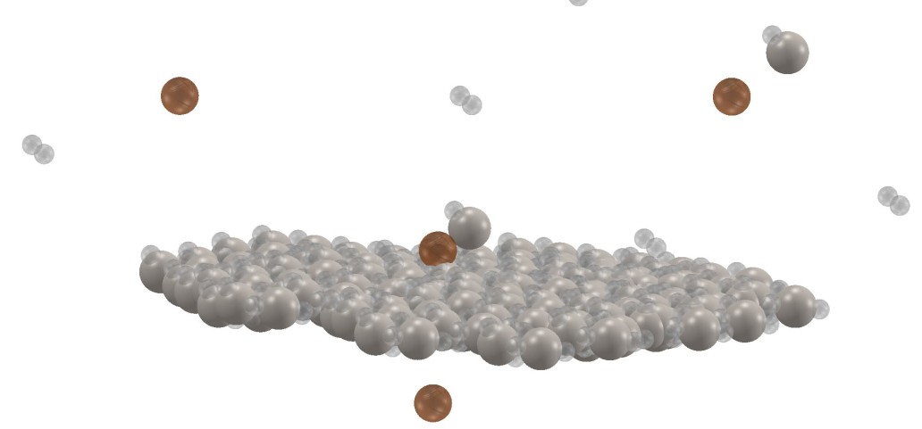
OCRICOM mainly focuses on vacuum deposition methods, which can crudely be divided into two main categories I. Physical Vapor Deposition (PVD) and II. Chemical Vapor Deposition (CVD). The number of subcategories is vast, and we shortly cover here only the most common ones that can be linked to our own work.
Chemical Vapor Deposition (CVD)
CVD produces thin films through chemical reactions of gaseous precursors at or near the substrate surface. CVD offers a versatile route to a wide range of materials and can be adapted to different substrate geometries, temperatures, and film requirements. CVD-based options that we can provide include atomic layer deposition, plasma-enhanced chemical vapor deposition, and diamond-like carbon coatings.
Atomic Layer Deposition (ALD)
ALD is a highly controlled, cyclic thin-film deposition technique based on sequential, self-limiting surface reactions (Fig. 1). It enables exceptionally precise thickness control and excellent conformality, making it particularly well suited for nanoscale coatings, surface passivation, and complex three-dimensional structures.
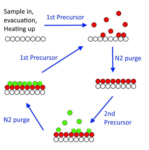
Figure 1. An illustration of an ALD film growth cycle.
With ALD one can readily deposit a large variety of materials, such as oxides, sulfides, nitrides, and even metals, on almost any type of surfaces. Our collaboration with SwissCluster enables us to provide you just the tool you need for your wanted ALD processes. Different ALD process options are available in SC Qube (Fig. 2), SC Optima and SC-1.
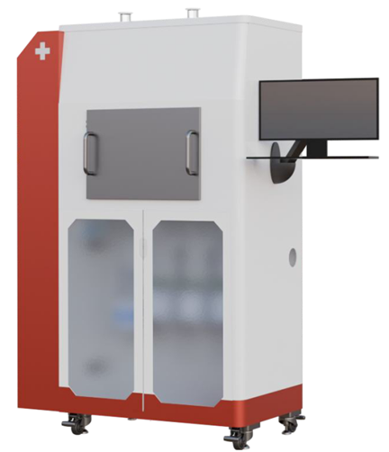
Figure 2. SC Qube platform that offers a large variety of possible processes starting from thermal ALD and ranging to FBR, and microwave plasma-ALD.
Plasma Enhanced Chemical Vapor Deposition (PECVD)
PECVD uses plasma to activate and enhance chemical reactions, enabling film deposition at lower substrate temperatures than conventional CVD. The method is widely used for depositing functional, protective, and optical thin films. Our capabilities with PECVD include mainly SiO2 or SiNx based RnD coatings/small batches, or a customized PECVD system for your needs. PECVD can be considered fast and dirty, in comparison to PVD methods and ALD, but in some processes it’s just what you need.
Diamond Like Carbon (DLC)
DLC-coatings are carbon-based thin films combining high hardness, low friction, chemical resistance, and optical properties that can be tailored through the deposition process. DLC can be deposited using plasma-assisted processes and is particularly attractive for protective and wear-resistant applications. From I-Photonics’ systems Diamanta is exclusively built to tackle DLC-processes for Si and Ge substrates.
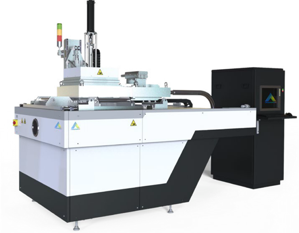
Figure 3. Diamanta platform designed for DLC-processes for infrared substrates such as silicon and germanium optics.
Physical Vapor Deposition (PVD)
PVD encompasses a broad range of vacuum-based thin-film deposition techniques in which material is physically vaporized from a solid source and transported through the vapor phase onto a substrate. PVD provides excellent control over film composition, thickness, and microstructure and is widely used for optical, protective, decorative, and functional coatings.
Electron Beam Evaporation (EBE)
EBE is a physical vapor deposition method in which an electron beam heats and evaporates a source material in vacuum. The resulting vapor condenses on the substrate to form a thin film. EBE is a versatile method for depositing a broad range of materials; almost anything that can be melted/sublimed in vacuum without decomposition/hazard reactions, can be deposit. Most common materials include oxides, fluorides, sulfides and metals. At OCRICOM we typically use EBE for metallic layers and coatings.
Ion Assisted Deposition (IAD)
IAD combines evaporation with simultaneous ion bombardment of the growing film. The ion assistance can improve film density, adhesion, mechanical properties, and environmental stability, while providing additional control over the resulting coating characteristics. It can also be used to deposit reactively materials that typically decompose while melted, such as nitride films. I-Photonics Ortus systems are built with IAD-processes for optical coatings in mind, and offer a versatile work-horse for any deposition lab needing their own thin film capabilities.
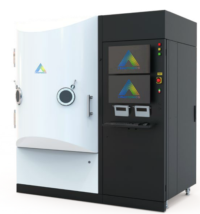
Figure 4. Ortus 700 evaporator designed with IAD capabilities for a large variety of EBE or thermal evaporation processes.
Ion Beam Sputtering/Deposition (IBS/IBD)
IBS, also referred to as IBD, is a highly controlled PVD technique in which an energetic ion beam sputters material from a target onto a substrate. Due to its energetic process, IBS deposition does not necessarily require additional heating for the substrates, which allows deposition also on heat sensitive surfaces. IBS produces dense, uniform, and highly durable thin films with excellent control over thickness and optical properties. It is particularly well suited for demanding optical coatings and precision photonics applications. Lidiz systems from I-Photonics are excellent IBS platforms built for high-quality laser optics and other challenging applications.
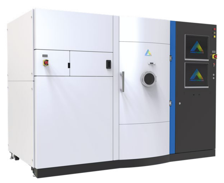
Figure 5. I-Photonics Lidiz-700 IBS with a load lock and in-situ broadband optical monitoring.
Magnetron Sputtering (MS)
MS is a versatile PVD technique in which plasma is used to sputter material from a target onto a substrate. Magnetic fields enhance plasma confinement near the target, enabling efficient deposition at relatively low pressures. Magnetron sputtering is suitable for a wide range of materials and applications, including optical, protective, and functional coatings. MS can be divided into several different categories based on the power source (DC, RF, pulsed-DC, HiPiMS), the process (direct, reactive, plasma-assisted), and their combinations. Via I-Photonics’ Meridian and SwissCluster’s SC-1, we can get you any kind of MS process tool you want.
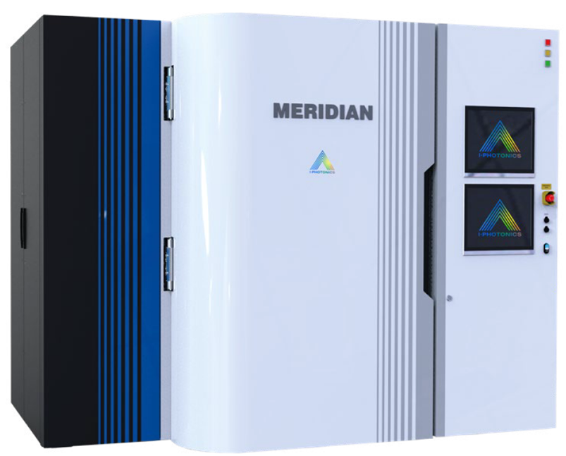
Figure 6. Meridian MS-platform specifically developed for challenging PARMS (plasma-assisted reactive MS), which can also be configured to other MS modes.
A combination of ALD/PVD
Combining ALD with PVD techniques provides capabilities that are difficult to achieve with either method alone. Hybrid processes combine the high deposition rate and material versatility of PVD with the exceptional thickness control and conformality of ALD, opening possibilities for advanced multilayer, functional, and optical thin-film structures. SwissCluster’s SC-1 is a novel small footprint system that combines ALD and PVD in a single tool without any needs for sample transfer or switching tools. It delivers process capabilities up to 300 mm diameter area with several unique features that are hard to realize with other tools.
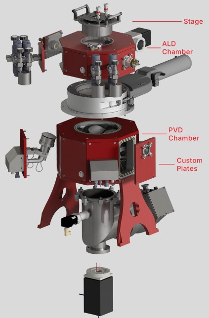
Figure 7. SwissCluster SC-1 is an innovative ALD/PVD tool that combines both methods in a single small footprint system, and does not require sample transfers.
OCRICOM’s work with the selected technology partners provides access to all of the presented deposition methods and systems. This allows us to select and combine deposition technologies according to the requirements of each application, from precision optical coatings and process development to advanced functional thin films and tailor the solution just for your needs. Ask to learn more!